
If you search for electron beam lithography definition online, most of the information you can explore explain that it has something to do with the artwork, mainly the ‘method for printing using the stone & a metal plate with entirely smooth surface’. Though, in the semiconductor industry, it is the procedure which is used for the device fabrication, the methodology which transfers the pattern from a photomask (also known as a reticle) to the surface of the substrate that is very valuable for the production of the electronic components like the integrated circuits.
The major factor of producing complex devices at a lower cost is lithography. There are several types of lithography – optical lithography has been reaching its physical limit & consequently leads to the development of alternate techniques. Immersion lithography has recently concerned interest in the research industry. In conclusion, we also inspect the potential of x-ray lithography and EBL as imaginable candidates.
Table of Contents
X-ray Lithography
The basic setup of a typical XRL system is by using the synchrotron as the x-ray source. Synchrotron-based XRL offers a wide exposure-dose window that is vital in ULSI fabrication. Insensitivity to dust is another advantage that will affect the number of pattern defects. The source is the electromagnetic wave that is produced when high-energy electrons are enhanced. To enhance the x-ray absorption, the mask substrate is made of a thin membrane that consists of materials with a low atomic number.
Immersion Lithography
This pushes the physical limits of NA for experience systems beyond NA=1 for air, given the following relation –
NA=n sin alpha = d/2f. Ultrapure water is extremely suitable as it has a refraction index of 1.47.
Electron beam lithography
The electron beam lithography system applies a direct writing technique to scan the electron beam across several material surfaces covered with the resist film to make desired widespread patterns on substrates. Because of the high-energy electron beam, it totally eliminates the diffraction effect; though, it can cause damage to the substrate material. The determination is now limited by the aberration of the electron optics & scattering effects that are more severe. Through scattering effect correction, it will reach a resolution of about 10-20 nm. As pattern generation is carried out via scanning surface pixel by pixel controlled by computer-aided design (CAD), it leads to slow speed, and thus very low throughput. Although this E-beam direct writing doesn’t need a mask that usually costs a lot for a specific material, delicate equipment costs & frequent maintenance are typically very expensive up to millions of dollars, so mass production is cautiously unfavorable. These speed & cost considerations limit its application in the mass commercial production of 50 nm feature size, though it has high level resolution. Instead, this technique is used to produce high-quality masks with good resolution & is also widely used for the research purpose. Of
There are several steps involved in the electron lithography procedure for semiconductor production. These are the following:
1). The imposition of structure on the beam – the lithographer imposes the structure on the beam of light, bypassing it through the ‘mask’ & this is followed by projecting the image to a silicon wafer coated with the thin layer of material known as the resist.
2). The chemical transformation – The resist covering substrate undergoes the chemical transformation when exposed to the light, a procedure which alters solubility of material & this alteration makes the latent pattern image to a patterned chemical stencil after application of the appropriate solvent.
3). The deposition – This can be a procedure where the substrate is placed inside the reactor, and a number of gasses are supplied that create a chemical reaction, producing the solid material with condenses on all surfaces inside the reactor.
4). The etching – The process which chemically removes the layers from the surface of the substrate; this process is required to pattern deposited layers – removing unwanted, leaving behind only desired traces & patterns.
Electron Beam Lithography is one of the powerful techniques for intending nanostructures that are very small to fabricate for conventional photolithography. State-of-the-art EBL systems can attain resolutions of a few nanometers. The technique works by moving the highly focused electron beam over the sample to write out the pattern intended with the appropriate CAD tools.
The pattern is also recognized in electron-sensitive film & resist deposited on the sample before experience by spin coating. The electron beam induces the change in the molecular structure and solubility of a resist film. Succeeding exposure to electron beam, this resist is established in an appropriate solvent to selectively dissolve either exposed & unexposed areas of resist.
Pattern transfer
After exposing & developing, the resist layer on top of a sample can be used as the mask or template for transferring patterns to a useful medium. There are widely two major pattern transfer techniques that can be applied – the first involves engraving material away beneath the voids in the resist layer, the second involves depositing layers of the material – usually metal – all over a sample, then liquefying away the remaining resist to “lift-off” the deposited material on top, leaving deposited material only in areas where there was no resist existent.
Supporting facilities
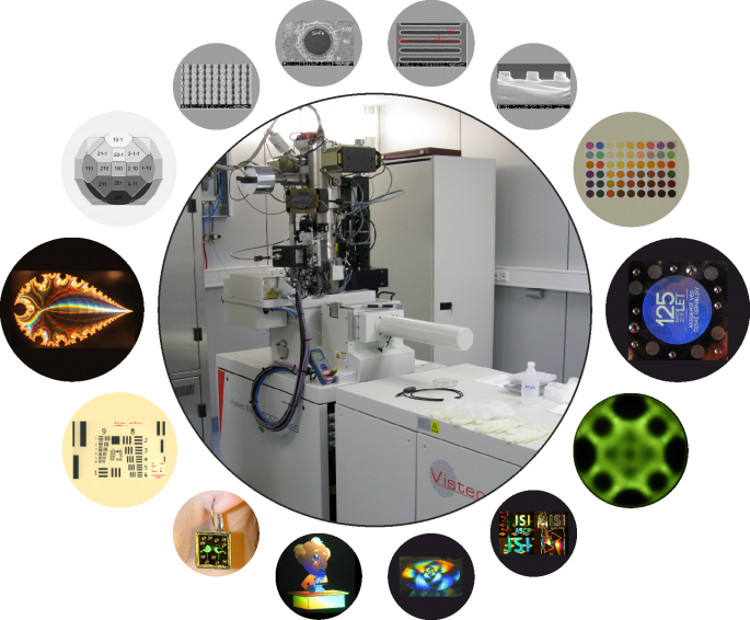
Users of electron beam lithography systems can access the comprehensive array of supporting fabrication & characterization systems based in Nanoscience & Technology Center clean rooms on the North Campus.
Most of the systems are a part of the National Epitaxy Facility, devoted to growing & fabricating III-V semiconductor devices and materials for the customer. Though, most of the fabrication & characterization facilities are obtainable to use on an array of other materials.
Fabrication:
- Substrate preparation that includes cleaving, ultrasonic bath, solvent cleaning, & plasma Asher.
- Resist developing & removal.
- Resist deposition that includes spin coasters & hotplates
- Sputter coating of the selected metals, such as Au, Ti, Ni, & Zn.
- Plasma enhanced chemical vapor deposition (PECVD) of Si3N4 & SiO2.
- A comprehensive array of chemical etchings.
- Reactive Ion Etchings.
- Bonding & device packaging.
- Inductively Coupled Plasma Etchings.
- Evaporators for depositing a wide array of metals & other materials.